Ohhh the beloved ESP series of micro controllers from Espressif! These little beauties (either the ESP8266 or the ESP32) are pretty amazing little devices. They can get just about any little job done that you want. I wanted to get my feet wet with Altium Designer. Up until this point I had never created my own schematic, board layout, or PCB. This is gonna be fun!
I had set out to focus purely on hardware, but really ended up getting into the entire product development cycle. I had a few goals in mind:
- Learn the basics of schematic creation
- Nets
- Part Definitions
- Connections
- Determine industry best practices for obtaining and/or creating part footprints
- Board Design
- Layout
- Part Placement
- Cutouts
- Learn how Altium handles routing
- Planes, Polygon pours and best practices
- Vias (blind, buried, and micro)
- Physical Parts
- Stencils and Solder Paste
- Part Placement
- Reflow Soldering
- Find the best online resources for PCB ordering
- This requires one to follow a manufacturing facilities guidelines 🙂
- Generate a Bill of Materials
- Enclosure
- Optimal Aesthtic
- Optimal Airflow for proper temperature sensing
- Software
- Tasmota Configuration
- Testing
Schematic
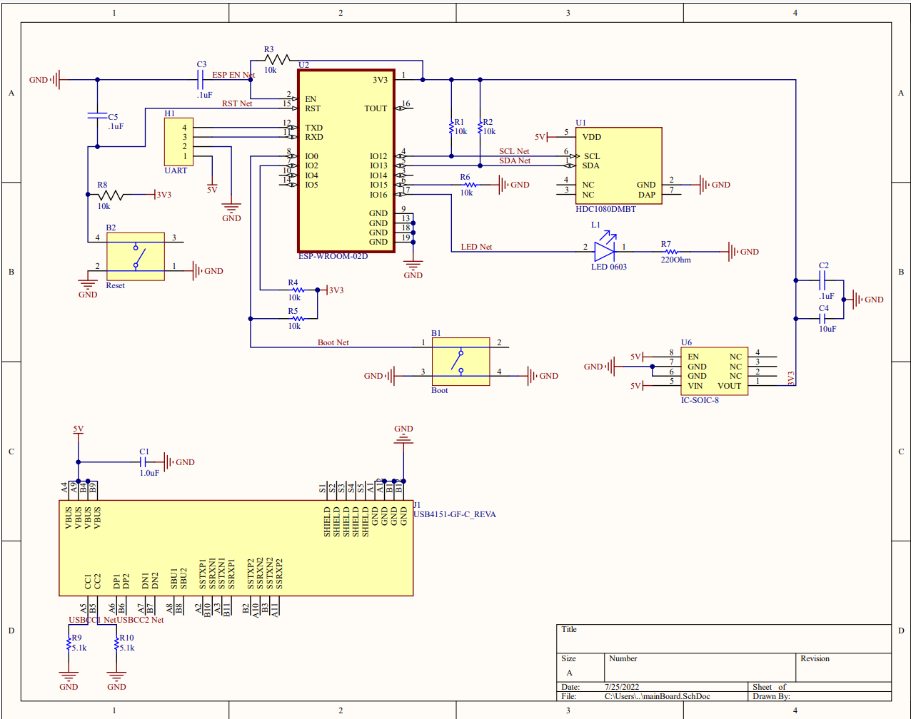
I absolutely loved searching for parts, reading datasheets, and ultimately finding just the right parts I need. Each section of the board needs its own specific implementation details met. Sites like Digikey, Mouser, Arrow, and Texas Instruments make finding parts incredibly easy. Most of them link directly to the parts schematic, and some will even give links to part footprints and 3d models that are already built and ready for you to use inside of Altium.
Part Placement and Routing in Altium
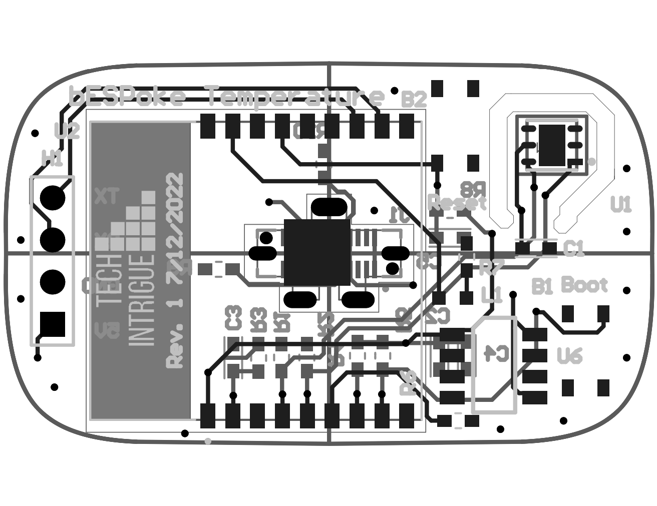
Routing is therapeutic. Finding an optimal route for a trace is like trying to solve a complex puzzle.
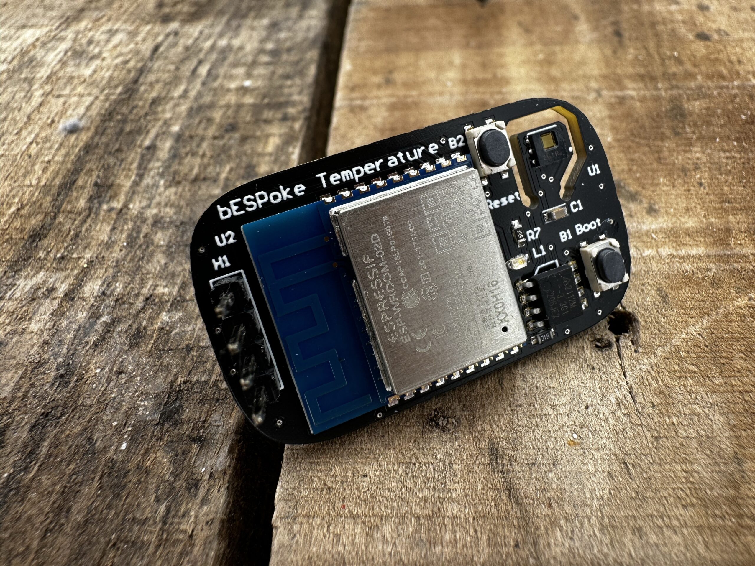
The HDC1080 from Texas Instruments is a high-precision digital humidity and temperature sensor that offers accurate and reliable environmental sensing capabilities. With its low power consumption, wide operating voltage range, small form factor, and robust performance, it is well-suited for a wide range of applications, including IoT devices which is perfect for this project.
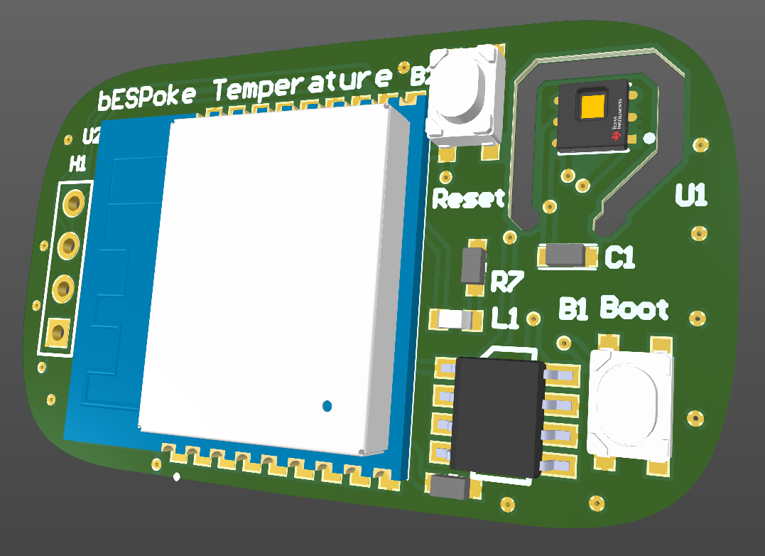
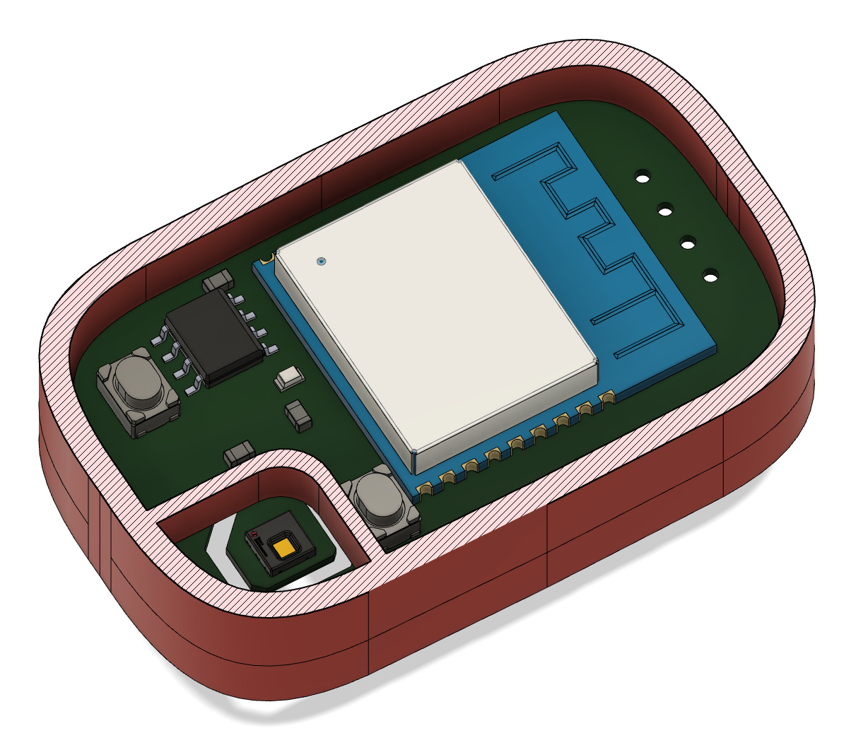
The cutout for the HDC1080 can be seen clearly here. This was recommended in the datasheet to help the accuracy of the sensor. I had my doubts on whether or not the cutout section would be strong enough. In the end, the PCB structure is more than adequate. The reset and boot buttons can also be seen here. The boot button is used to put the ESP into programming mode. Section H1 is the header for a UART connection to program the ESP module.
The LDO Linear Regulator(AP2112) that converts our 5v USB to 3.3v can also be seen. I chose the LDO regulator for a number of reasons, including but not limited to the following.
The diode in the AP2112 serves as a protection mechanism, allowing current to flow in only one direction. This helps prevent reverse current flow, which can occur when there is a voltage higher than the output voltage applied to the output terminal of the voltage regulator. Reverse current can potentially damage the circuitry or the load connected to the output of the voltage regulator, and the diode in the AP2112 helps mitigate this risk.
Additionally, the diode in the AP2112 also provides a path for discharging the output capacitor when the input voltage is removed, helping to quickly discharge any stored charge and ensure a rapid power-down of the regulator.
Overall, the inclusion of a diode in the AP2112 helps enhance the functionality and protection of the voltage regulator.
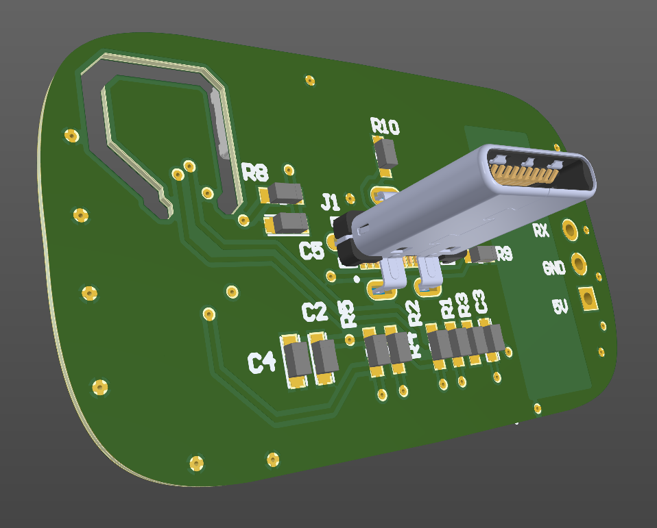
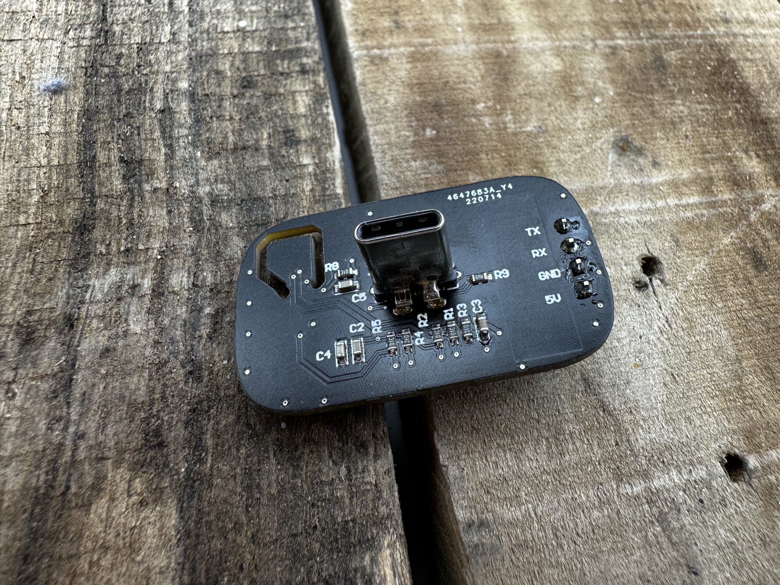
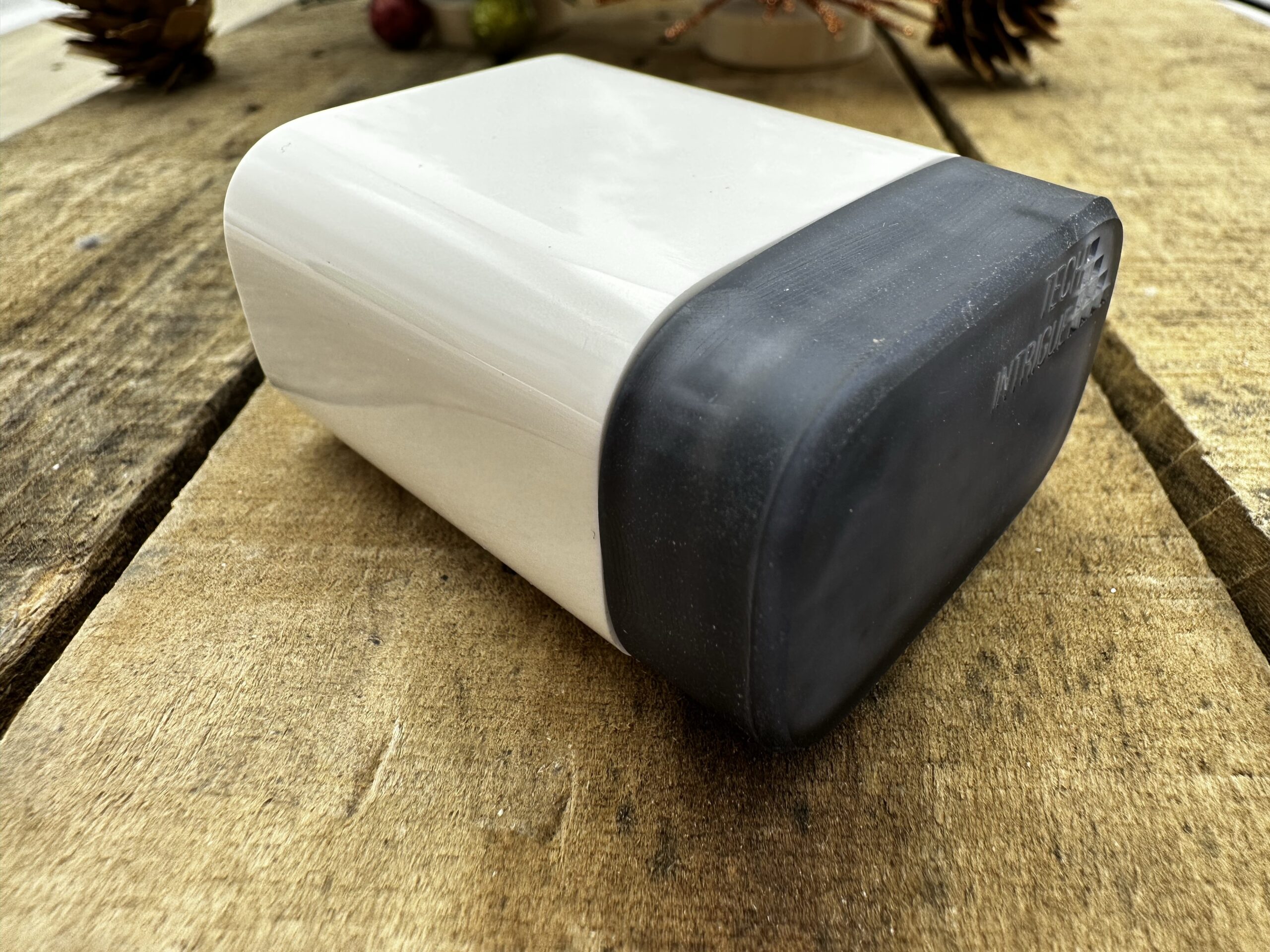
The 90 degree male USB-C connector is possibly one of the most interesting parts of this PCB design. It is mounted directly behind the ESP32 chip on the other side, this was necessary to mount seamlessly with the Apple USB-C charger. Altium did not like this part being in this position as it saw many collisions, but the familiarity I had with these parts over the month of design made me confident that this would work.
PCB and Part Placement on the Physical PCB
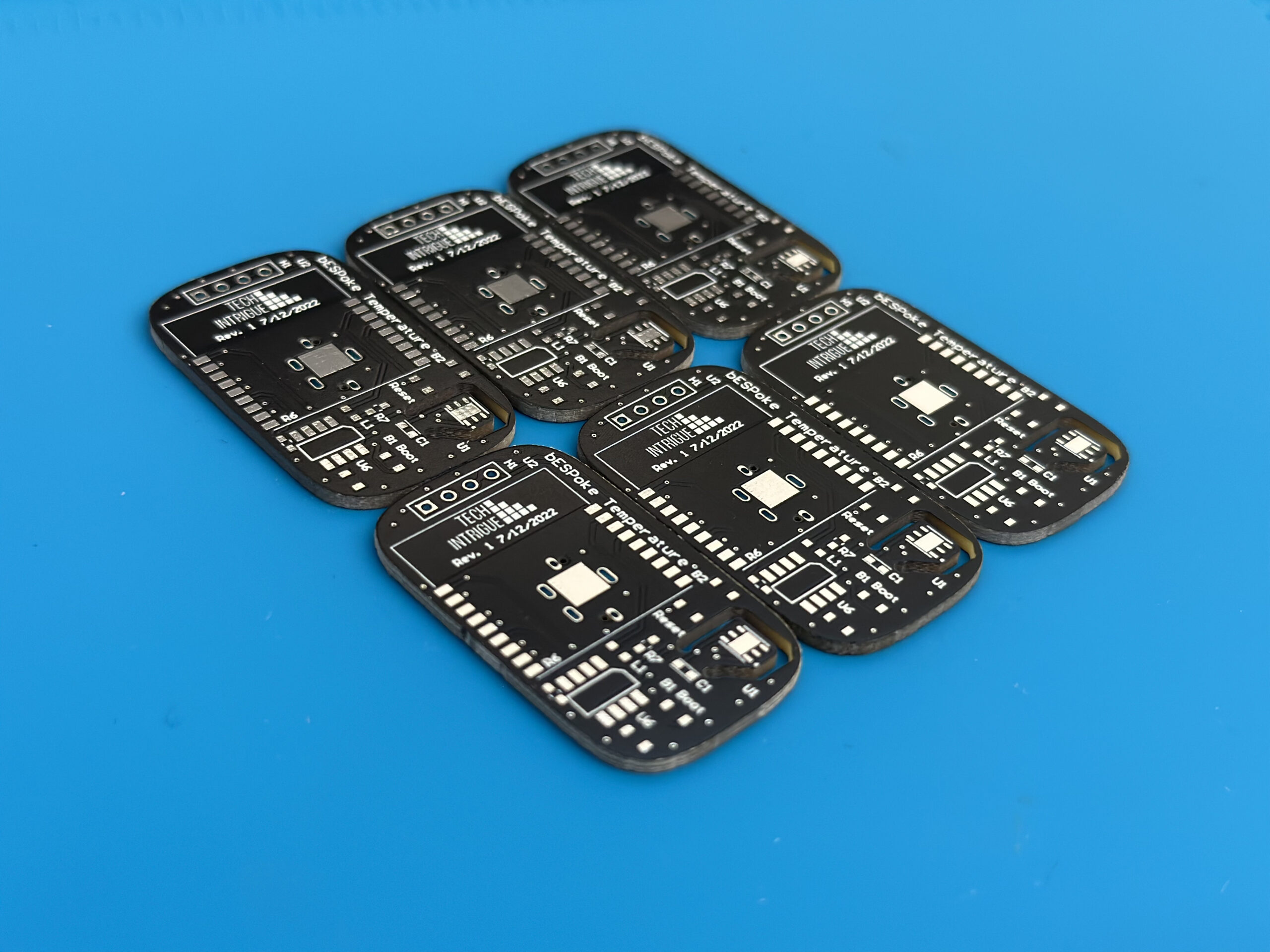
Raw boards from the board shop. Everything is looking really nice at this point!
The board shop has an option to provide a stencil which I vouched for. Along with the stencil comes a digital file (DXF) of the stencil. The DXF along with the digital rendering of the board from Altium allowed me to create a stencil jig that gave me a perfect template to apply solder.
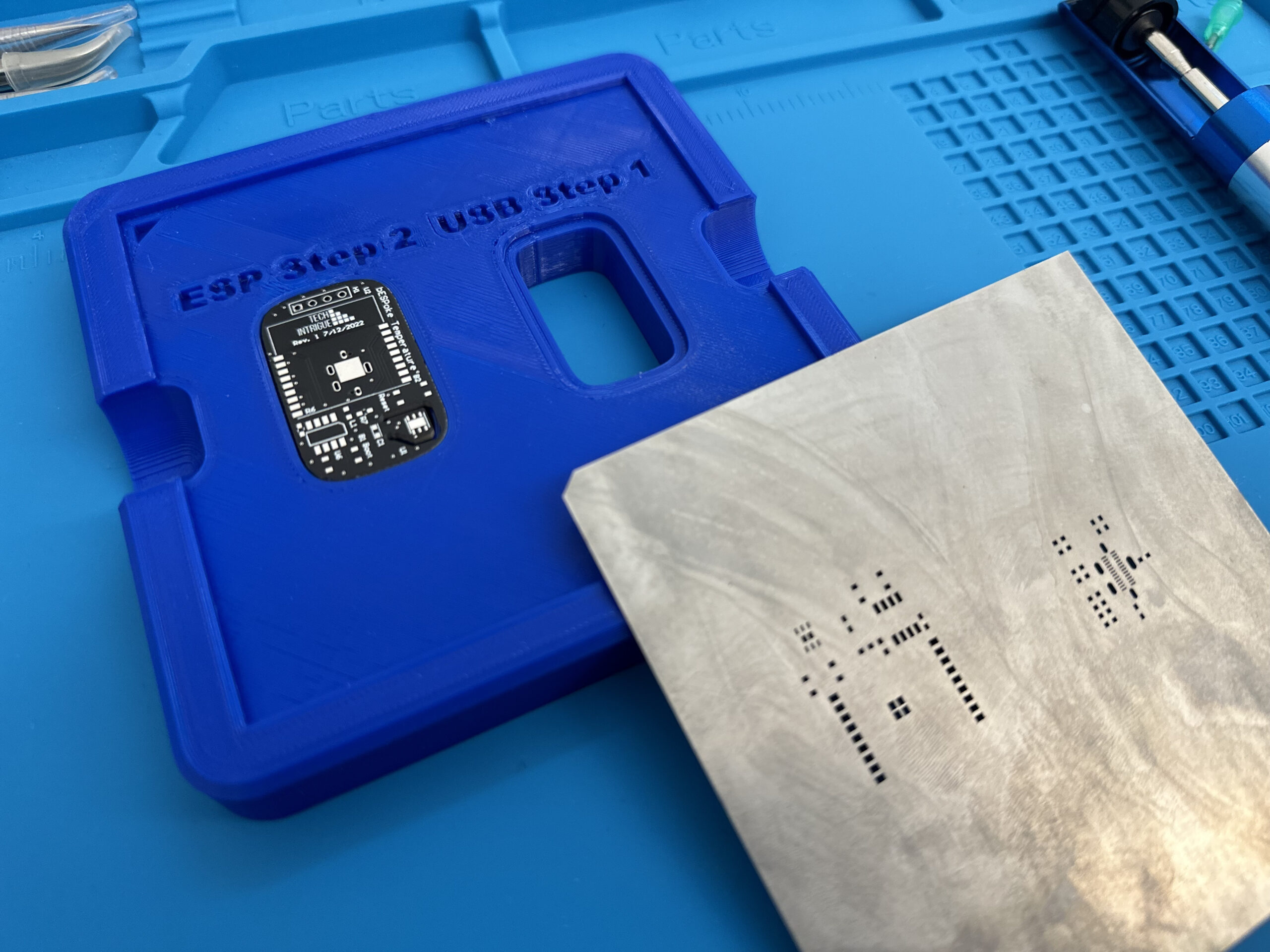
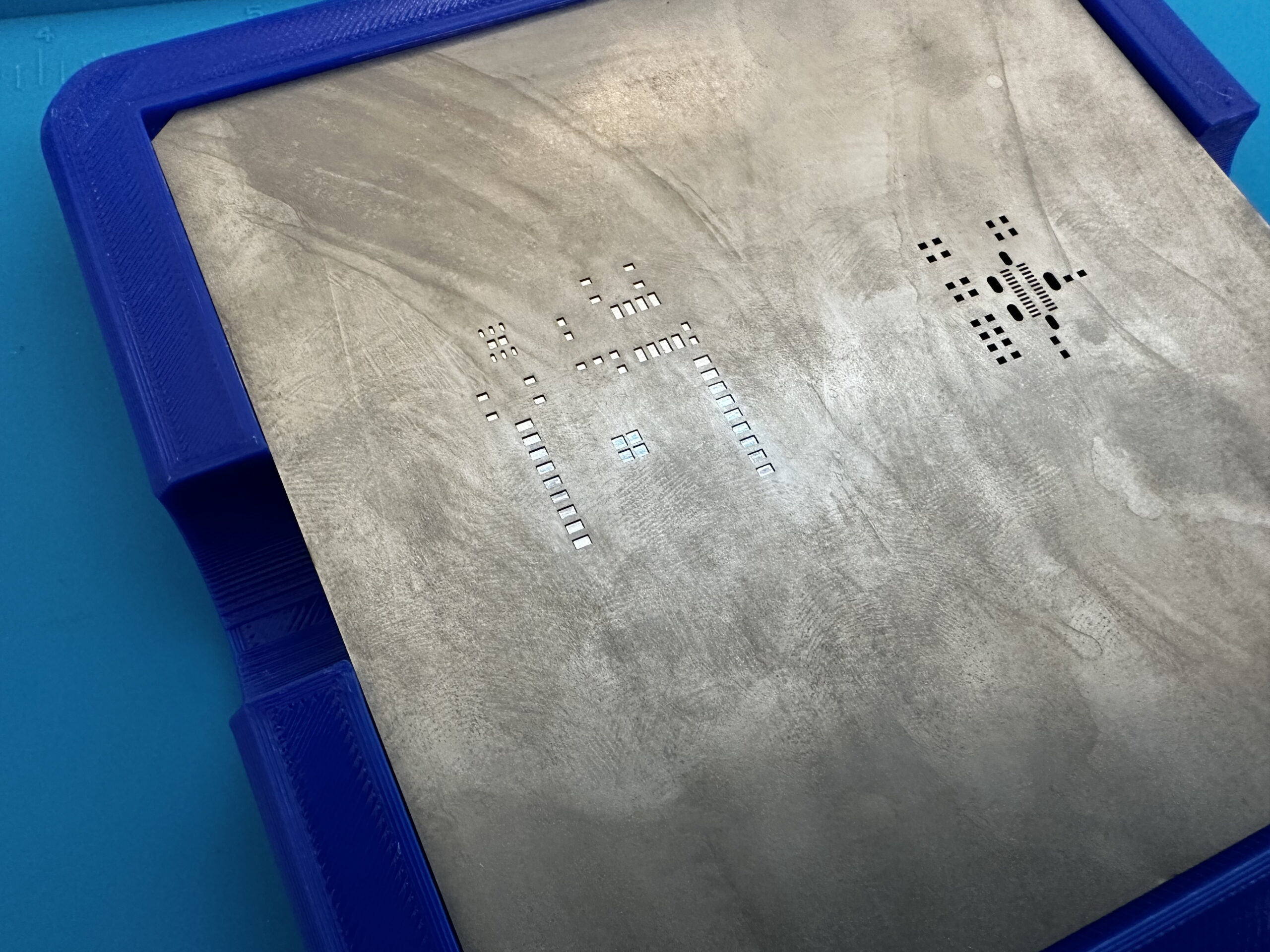
As you can see here, the stencil aligns perfectly with the pads for all of my parts.
Soldering Oven
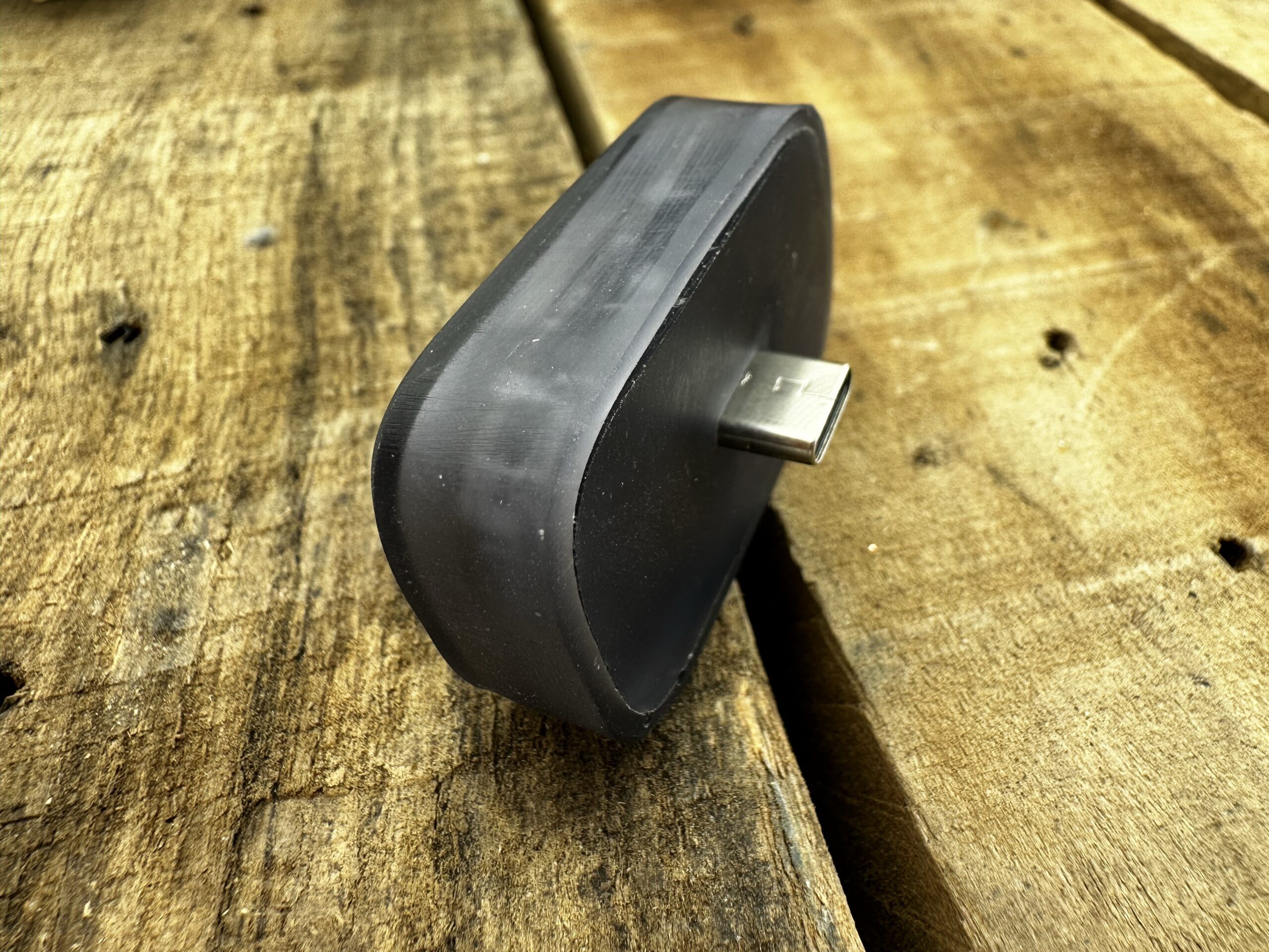
The final PCB with parts turned out better than I could have ever expected. I am thrilled that my design has worked up to this point!
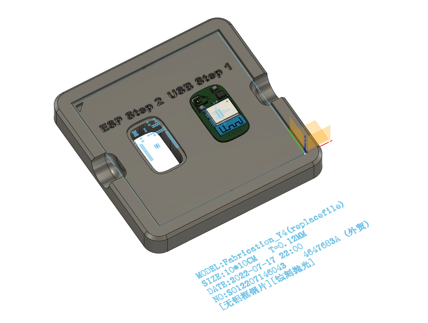
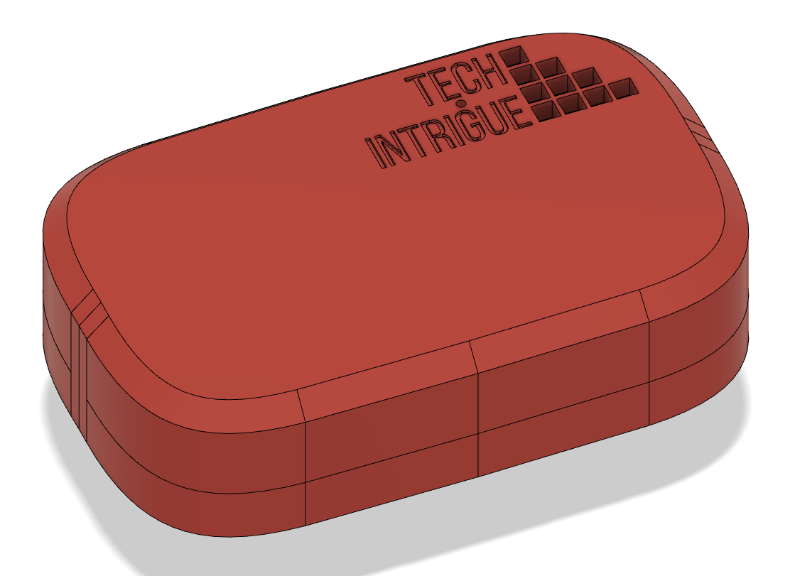
Enclosure Design
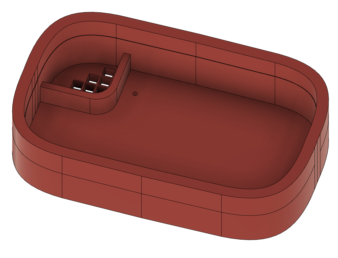
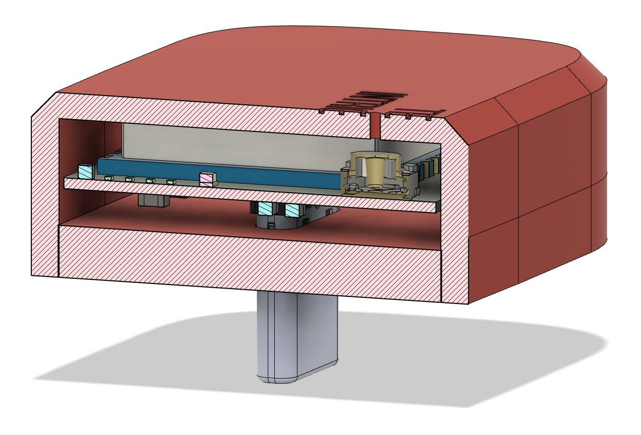
A special partition was created inside the top section of the enclosure to help create a clean temperature zone.
You can see in the cross section the HDC has its own special place within the enclosure.
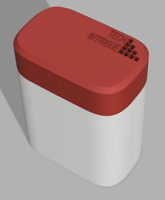
A rendering of the enclosure attached to the Apple USB C power brick.
Enclosure and Final Aesthetic
0 Comments